Table of Contents
My writeup on IBM 1401 core memory: the epic
From Ken Shirriff < ken.shirriff@gmail.com >
Core memory in the IBM 1401
The IBM 1401, like most computers of its era, uses ferrite core memory, which was the leading memory technology from the mid-1950s until it was replaced by semiconductor memory in the early 1970s. For its time, core memory provided relatively dense, reliable, and inexpensive storage.The 1401's main core memory provides 4,000 characters of storage, as well as special I/O storage. Each bit of data in memory is stored in a tiny ferrite ring or core. These cores can be magnetized in one of two directions, corresponding to a 0 or 1 bit. The cores are arranged into a grid of 4000 cores, called a plane. Each plane stores one bit of a character, so 8 planes are stacked up to store a character. (The additional I/O planes will be discussed later.)
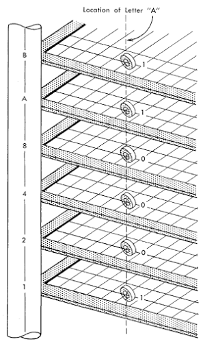
The diagram below, from the 1401 Reference Manual illustrates how the character 'A' is stored in core memory. To select an address, an X wire and a Y wire are activated, selecting the cores where those two wires cross. The bits from the selected location each plane make up the character. Since there are 4000 cores in each plane, the core module provides 4000 characters of storage.
Properties of ferrite cores
The physical properties of ferrite cores are critical to the operation of the core memory, so it is important to understand them. First, if a wire through a core carries a strong current, the core will be magnetized according to the direction of the current (following the
right-hand rule).
Current in one direction will write a 1 to the core, while the opposite current will cause the opposite magnetization and write a 0 to the core.
Hysteres is is a key
property of the cores: current must exceed a threshold to affect a core's magnetization. A small current will have no effect on the core, but a current above a threshold will cause the core to "snap" into the magnetized state aligned with the current.
The hysteresis property makes it possible to select a particular core. A "half-write" current is sent through the appropriate X select wire and a "half-write" current through the Y select wire. The single core with the selected X and Y wires will have enough current to change state, but the other cores will not have enough current, and will remain unchanged.
The final important property is that when a core switches its direction of magnetization, it induces a current in a sense wire through the core (kind of like a transformer). If the core already has the target state and doesn't change magnetization, no current is induced. This induced current is used to read the state of a core. A consequence is that reading a core erases it, and the desired value must be written back to the core.
To write a core, current of the opposite polarity is sent through the X and Y select lines to magnetize the core into the 1 state. To keep the core in the 0 state, a current is sent through the plane's inhibit line. The inhibit wire runs through all the cores in a plane parallel to the X select lines. By running the reverse current through the inhibit wire, the X line's current is canceled out, and the core remains unchanged. The inhibit current is too low to flip a core by itself, so other cores are not zeroed out. Each plane has an inhibit wire threaded through all the cores in the plane, so the appropriate value can be written to each plane.
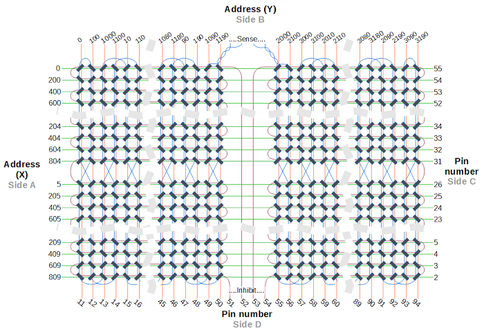
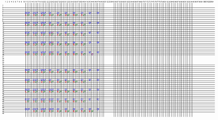
The diagram below shows the reverse-engineered wiring topology of a IBM 1401 core memory plane. Most of the core has been cut out of the diagram, as indicated by the dotted gray lines. The sides of the plane are labeled A through D, matching the 1401 documentation. The A and C sides have 56 pins, while the B and D sides of the plane have 104 pins. Not all the pins are connected.
Each half of the core plane (0-1999 and 2000-3999) has a separate sense line loop, but they are usually wired together. The two sense lines are in blue and run in the Y direction. The sense lines are carefully arranged to avoid picking up interference. The lines cross over along the midpoint to cancel out noise from the Y select lines - the sense line runs in the opposite direction along half of each Y select line, so any induced signal will be canceled out. In addition, the sense lines are twisted as they exit the middle of the plane, to avoid picking up interference. (Many other core memory systems avoid interference by running the sense line diagonally, but the 1401 uses a rectangular layout.)
Each half of the plane has a separate inhibit line. The two inhibit lines are in brown and run next to the X select lines, which they inhibit. The two lines are normally driven separately to reduce noise, but have the same signal. Since the inhibit line switches direction each row, alternating X select lines are also driven in opposite directions.
Address decoding for the core module is fairly complex. The tens digit is decoded into ten separate input lines (0 through 9), as is the units digit. The hundreds digit is split into the three top bits (called "even hundreds") and the low-order bit (called "odd hundreds"). The value of the even hundreds generates five input lines: 0, 2, 4, 6, and 8. The odd hundreds generates two input lines: 0 or 1.
The X and Y select lines is output by a matrix switches. Each matrix switch takes two sets of input lines and activates an output line based on the input values. The X matrix switch has the 5 even hundreds lines as one input and 10 units digit lines as the second input. There are 50 combinations of inputs, so the X matrix switch has 50 outputs, which are used as the X select lines. For the Y matrix switch, the thousands (4 values) and odd hundreds (2 values) are combined to yield 8 input lines. The second Y input is 10 tens digit lines. The output from the Y matrix switch activates one of the 80 Y select lines. This addressing mechanism may seem overly complicated, but it minimizes the hardware required for address decoding.
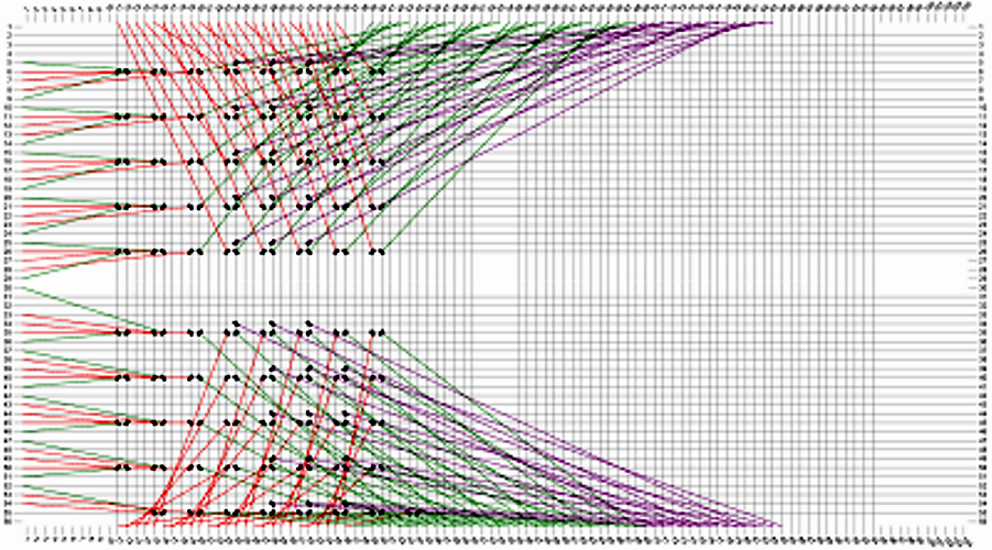
Two bundles of wires connect to I/O planes near the middle of the module. One connects the brushes in the card reader and the printer hammer drivers to terminals on frame 11, which are connected to the cores in frame 12. The other bundle connects read brushes and punch check brushes to terminals on frame 9, connected to the cores in frame 10. In between, short horizontal yellow wires in the middle jumper the Y select lines across frame 11. The horizontal wire bundle across the middle of the planes connects to the inhibit lines of each plane.
The photo below provides another view, focusing on the data plane wiring. At front is frame 1, the core plane for data bit 8. The gray cores are visible on red wires. The other 15 frames are layered behind frame 1. At top is side D of the module, with the two matrix switches on top. The 8x10 matrix switch is connected to the Y select lines at the front and back of side D. These wires alternate with black wires that connect the select lines to termination resistors. The 5x10 matrix switch is connected to the X select lines at the front and back of side C, on the left. This side also has jumpers between planes to connect the X select lines.
The I/O planes are addressed exactly the same as the data planes, and share the X/Y select wires. However, the I/O planes are very sparse, with only 297 cores rather than 4000 cores, so most locations have no storage, as can be seen in the photo below.
The first direct-wired plane is frame 10, which holds data from read station 2 brushes (RD2) and the punch check brushes (PCH). The second direct-wired plane is frame 12, which holds data from read station 1 brushes (RD1) and the print hammers (PRT). As a card passes through the card reader, 80 brushes check each position in a row. If there is a hole, the brush makes connection passing a current through a wire connected directly from the card reader to the core module. Each wire from a brush is wrapped around the corresponding core, so the core is set to 1 if a hole is present. Since there are three read stations with 80 brushes each, there are 240 wires between the reader/punch and the core module. Each of the 240 brushes is wired directly to a separate core. There is no buffering or driver between the brush and the core, just a direct wire that is wrapped five times around the core and connected to a -20V common wire.
(Field Engineering page 95 and
(ALD 42.40.51.1.)
The print hammer cores are also wired individually. Each of the 132 hammer driver is connected directly to a core to record the operation of the hammer. After passing through a core, each of these 132 wires is connected to a -60V common wire.
(Field engineering manual, page 107,
ALD 42.40.52.1 and
36.38.61.2-36.39.91.2.)
Because of the large number of I/O wires that must be connected and routed, separate terminal frames are used above the core frames. Frame 9 provides the terminals for the cores in frame 10, and frame 11 provides the terminals in frame 12. That is, frames 10 and 12 have the cores along with select, sense, and inhibit lines, while the brush and hammer wires are connected to frames 9 and 11, which then have the wires wrapped around cores in frames 10 and 12. The -20V and -60V common wires are internal to the frames.
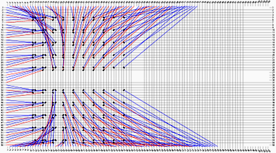
The following diagram shows how the terminals in frame 9 are wired to cores in frame 10. Read indicates read 2 brushes, greeen indicates punch check brushes, and purple indicates 1404 read brushes (unused).
During the card read process, a pair of planes (XU/XL) or (YU/YL) counts the holes in each column at the first read station. This count is verified at the second read station; if the counts don't match, the read fails. For punches, the counts are verified against the expected number of holes. (It's not exactly a count; XU or YU tracks the presence of any hole, and XL or YL maintains the parity of the count.) Because one card is being read/punched while a second is being verified, two counts must be maintained. Alternate cards switch between XU/XL and YU/YL.
(ILD page 62).
Printing uses print-compare cores in the XU plane. These are set if a hammer should fire for the character position. These are compared with the hammer-fire cores (set by the hammer drivers) to verify that the correct hammers fired. Plane YL holds print-line complete cores that verify that every character position either printed a character or holds a non-printable character. If a core is not set, something went wrong with the printing logic. Finally, area YU has print-error storage cores. If a print error is detected, the corresponding core is set, allowing the location of the fault to be dumped out.
(ILD page 72 and
Data Flow pages 62-63.) When the optional Print Storage feature is installed, the Print Storage core module is used instead of these planes.
The read operation starts with the input pulses to the matrix switches. The X matrix switch inputs are gated by timing signals R1 (000-036) and R2 (008-075), and the matrix generates a read pulse for 007-035. The Y matrix switch inputs are controlled by timing signals R1 (000-036) and R3 (015-075). The Y matrix generates a read pulse for time 015-035. These read pulses select the desired cores in storage, possibly triggering signals on the sense lines. The sense amplifiers are gated by Strobe A 014-030 to read the value from the cores. The value is stored in the B register, which was cleared from 000-015.
The read operation is followed by the write operation. The write timing signals Z1 and Z2 (068-105) activate the inhibit drivers. The write is triggered by the negative-phase select pulses from the matrix switches, generated when the switch core resets from 070-000. Thus, the write finishes just at the end of the machine cycle, in time for the next cycle.
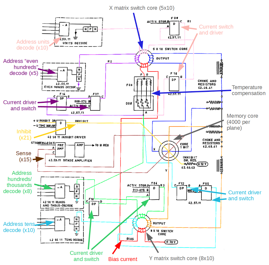
The diagram below annotates the
Switch Core Circuitry diagram.
It shows in detail the circuitry used to drive one of the 4000 cores in a plane. The notation in this diagram may be confusing. The rectangles indicate SMS cards. The letter inside the rectangle indicates the function:A is an AND gate, DP is a current driver, and D is a switched driver. The text above an SMS rectangle ("F 14") is the position of the card in gate 01A1. The letters outside the box ("A", "B", "C") are pins on the card. The numbers ("42.57.11") indicate the relevant ALD. R1 and R2 are read time signals. Numbers ("014-030") indicate a timing signal.
The brown line shows one of the sense line circuits, driving a sense pre-amp and amplifier, and then feeding the B register.
The red line shows the bias current which passes through all the matrix switch cores. The properties of ferrite cores change with temperature, so the current is adjusted by a temperature compensation circuit (an
AKB thermal switch card and an
AKC memory emitter resistor card).
This current then splits four ways, going to the X matrix decode drive lines (pink and purple) and the Y matrix decode drive lines (green and cyan). Note that only one switch core from each switch matrix is shown.
The outputs from the matrix switches (blue and orange) are the select lines that go through the cores and are terminated by chokes (inductors) and resistors. Only one of the 50 X select lines and one of the 80 Y select lines are shown.
To write a character back to storage, the 1401 generates 8 inhibit drive lines: bits 1, 2, 4, 8, A, B, check, and word mark. These lines are generated by selecting from the A register, B register, manual console entry, arithmetic value, or expanded edit
(ILD page 10). However, these inhibit lines do not go directly to the core planes. Instead the data planes are split in half and each half has separate inhibit drivers and inhibit lines. The planes are split into addresses 0-1999 and 2000-3999, but both halves receive the same inhibit value. The motivation of the split is to reduce sense noise. (See
Optional Feature pages 6 and 7.)
The I/O planes have their own inhibit drives, and each plane has a single inhibit line. The XU, YU, XL, and YL check planes have inhibit drives that are generated by the hole counting circuitry in the reader / punch circuit
(ILD page 62).
The RD1-PRT plane and RD2-PCH planes are not written under computer control, but by the individual wires from the brushes or hammers to the cores. Thus, the inhibit signal for these planes is always activated for writes, and a read/write cycle clears the cores to 0. A single inhibit driver provides the inhibit signal for both planes; the inhibit lines for the planes are connected by a jumper between frame 10 and frame 12
(ALD 42.40.43.2).
The PRT cores do not have any inhibit, so they are set to 1 at the end of a read/write cycle. When a hammer fires, the associated core is set to 0 by the direct wire.
The inhibit lines are driven by
AQV driver cards, which provide the necessary current
(ALD 42.50.11.2).
There are 13 termination resistors for the inhibit lines on a termination board. The split inhibit lines for the data lines share termination resistors even though they have separate drivers
(ALD 42.40.43.2).
The sense line forms a loop through the cores in a plane, with both ends of the loop terminating at a
WX differential pre-amplifier card,
The pre-amplifier is somewhat different from a modern differential amplifier in that it is symmetrical and gives a positive output for handles a pulse of either polarity. The pre-amp is strobed at time 014-030, to read the sense line during the read pulse. The output of the pre-amplifier goes to the
AQX final amplifier and then to the
logic circuit that uses this bit.
For the data planes, the sense lines in the two half-planes are wired together to make 4K planes. Each I/O plane has a single sense line through the populated cores. An exception is frame 10, which has separate sense lines for the RD2 cores and the PCH cores.
The sense circuitry is described in
ALD 42.59.11.2 and
ILD page 4.
The 1401 uses an interesting solution to drive the select signals. Matrix switches generate the select signals by using a set of ferrite cores. But instead of storage, these cores are used for their switching properties. As with storage, the matrix switch depends on the "coincident current" property, where two signals of sufficient current will cause a core to snap to the opposite magnetization. But instead of being used for storage, the cores in the matrix switch generate a drive signal.
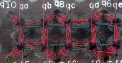
The photo below shows the wiring of the matrix switch cores. The bias wire (black) is wound through pairs of cores three times. Each horizontal input wire (red) is wound through pairs of cores about twelve times, as are the vertical input wires. Since the bias current is four times the input current, the winding numbers ensure that the bias cancels one input: two inputs will set the core, one input will have no effect, and no inputs will reset the set core (due to the bias current). Each core has an output wire wound diagonally about twelve times.
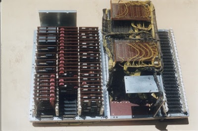
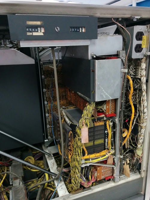
The photo below shows the core module mounted inside the IBM 1401 mainframe, looking into the left end of the computer. The core module is behind the bundle of black and yellow wires, mostly address lines. The matrix switches are on the left. The colorful brush and hammer wires are connected via paddles underneath the core module. The SMS driver cards are above the core module, mostly behind a metal cover for airflow.
The photo shows some other interesting features of the 1401. At the top of the computer is the time meter used for billing, measuring the time the computer has been running; customer time is on the left and unbilled maintenance time is on the right. In the upper right is the "convenience" outlet located inside the computer. At the far right is the wiring on the back of the front console. Unlike most of the gates in the IBM 1401, the core gate does not swing out, but is screwed into place. Other gates are visible behind the core module, and to the left.
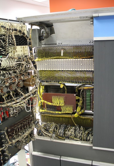
The back of the core module can be accessed by opening the computer's front panel, as seen below. The console switches, lights, and wiring are on the left. The core module itself is in the center, mostly hidden behind the brown termination resistor circuit board.
Structure of a core plane
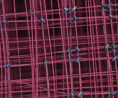
Each core plane has 4000 cores arranged as a 50x80 grid of cores. (The I/O planes are configured differently, and will be explained later.) To reduce interference, the ferrite cores are arranged in a "checkerboard" pattern with each core arranged diagonally in the opposite direction from its neighbors. Four wires pass through each core. The horizontal wires are the X select line and the inhibit line (used for writing). The vertical wires are the Y select line and the sense line (used for reading). The X and Y select lines go through all the planes, so all planes are accessed in parallel.
To read a core, the X and Y select lines magnetize the selected cores to the "0" direction. If the core was previously in the "1" state, the core's state change induces a current in the sense wire. If the core was already in the "0" state, no current is induced. Thus, the sense wire allows the bit stored in the core is determined. The read process destroys the previous value of the core, leaving it in the 0 state. Each plane has a sense wire threaded through all the cores in the plane.
The X select lines are in green and the Y select lines are in red. The select lines are generated in a complex way (described below), so cores are not arranged sequentially. To find the address of a core on this diagram, add the labels on the X and Y select lines.
Address decoding
The IBM 1401 uses a three-character address to access 4000 locations (addresses above 4000 will be ignored for now.) The decimal parts of the three characters specify the address from 000 to 999. The two zone bits of the hundreds character provide the thousands digit 0 to 3.
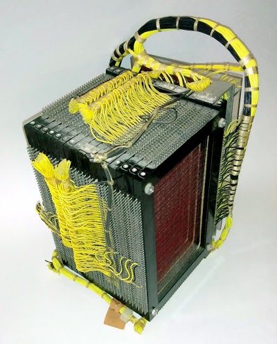
Physical layout of the core module
The core module consists of 16 frames - 14 core planes and two terminal planes. The first 8 frames hold the character data planes. The next 8 frames are used for I/O. The frames are stacked to form the core module. The following table shows the usage of each frame:
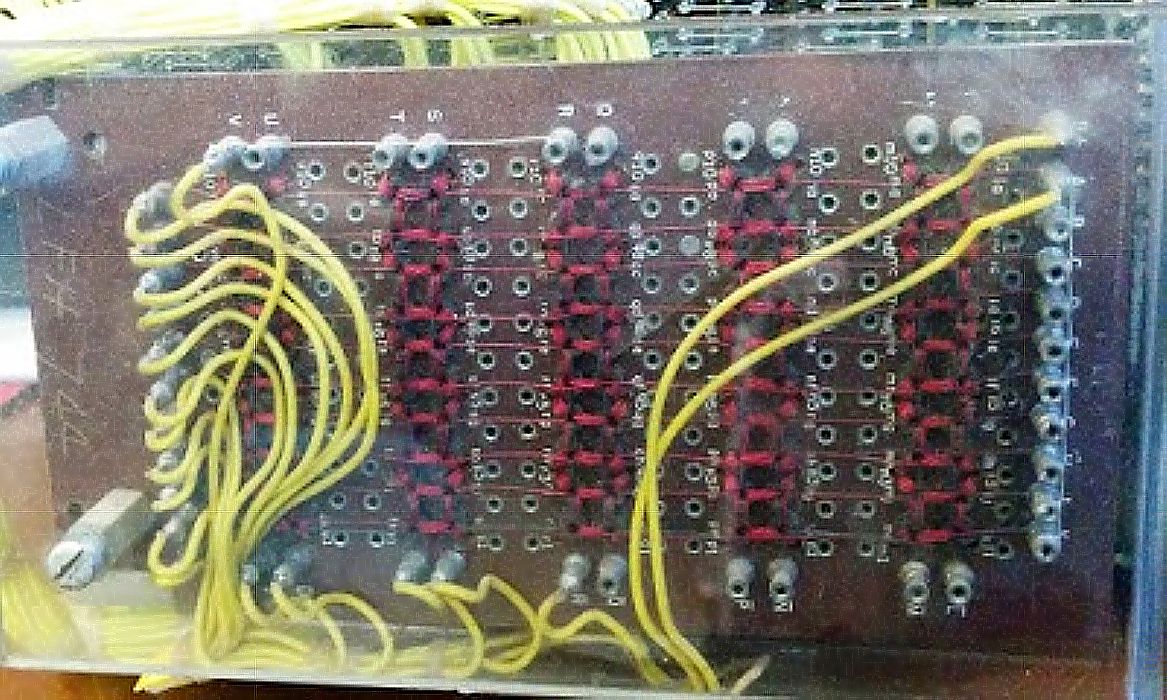
The picture below shows one side of the core module, side D, showing the large amount of wiring required. Frame 16 (YL) is at the left and frame 1 (bit 8) is at the right. The two matrix switches are on the front of the module: the 8x10 switch for the Y select lines is at top, and the 5x10 switch for the X select lines is at the bottom.
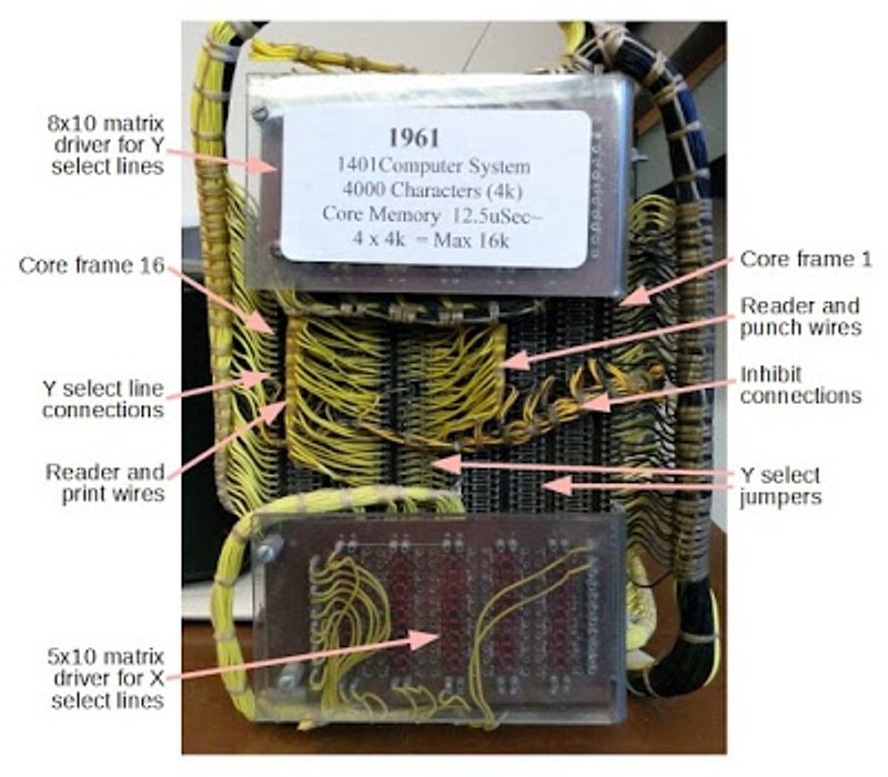
Much of the wiring in this picture is for the Y select lines, which flow through all the planes. The yellow wires at the left connect the Y select lines on frame 16 to the 8x10 matrix switch or termination resistors. The horizontal Y select jumpers are barely visible; they connect pairs of planes, allowing the Y select lines to flow through the whole module. At the far right, the Y select lines of frame 1 are connected to the 8x10 matrix switch and termination resistors.
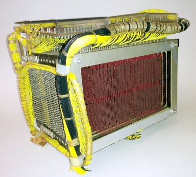
The photo below shows the other sides of the core module, focusing on the I/O wiring. On the right is frame 16, one of the hole count frames. This frame only has 297 cores. At the top is side A, with wires from the read brushes, punch check brushes, and print hammers wired directly to cores in frames 10 and 12. At the left is side B, which also has wires from the read brushes, punch check brushes, and print hammers. The two wires connected to the middle of side B of each frame are the sense wire connections.
The I/O frames
One unusual feature of the core module is the eight special-purpose I/O frames: six core planes and two terminal frames. These planes have multiple uses. They hold 80 positions of data when a row is read during card reading or punch checking. They are used for validity checking during card reading, card punching, and printing.
The planes have cores at addresses 1 to 80 for reading, 101 to 180 for punching, and 200 to 332 for printing. Inexplicably, there are also cores at addresses 185, 335, 336, and 337. The diagram below shows the layout of I/O cores. Read cores are red, punch cores are green, print cores are blue, and other cores are purple.
The I/O planes are not read and written like data planes. While they are addressed in parallel with the data planes, data read from these planes goes to the appropriate I/O circuitry, rather than the regular data path. Four of the planes have values written by the I/O circuitry. Two planes have individual cores wired to read brushes or print hammers, so the cores are modified directly; they are not written using the normal core addressing / inhibit circuitry. The other four planes are written by I/O circuitry in the 1401.
The following diagram shows the wiring between frame 11 and the cores in frame 12. Red indicates read 1 brushes and blue indicates hammers.
The four remaining I/O planes are XU 11, YU 12, XL 13, and YL 14 (frames 13 to 16). These planes are used for read/punch hole counting and for print validity checks.
Core memory timing
The IBM 1401 has an 11.5 microsecond machine cycle, which corresponds to one core read/write cycle. When describing the circuitry, however, the machine cycle is rounded to 12 microseconds for convenience. Timing is described in units of 0.1 microseconds, so each cycle has a time value from 000 to 120. Each cycle is broken into eight clock phases of 015 units (1.5 microseconds). For example, a time interval can be denoted as 045-060. Note that these times are about 4% off from the real time values. Some timing signals, including core timing controls, are not aligned on intervals of 015; they are generated from a
CEA delay card. [Delay Line Lumped, 1 Usec] (
ILD page 1.)
The core module circuitry
The detailed diagram below is the key to understanding the 1401's core memory system and is worth close study. This diagram (
ALD 42.41.11.2)
shows the physical arrangement of the 16 frames in the core memory module, along with the driver circuitry. The inhibit drivers are at the upper left, feeding each core plane. The sense amplifiers are at the upper right. The 5x10 X matrix switch is in the lower left, and the 8x10 Y matrix switch is in the lower right. Note the read brushes, punch brushes, and print hammer drivers are wired directly into the core module through the terminal frames. The "IS" and "ID" boxes feeding the matrix switch are the current source (buffer cards) and current drain (switch cards) driving the matrix switch, respectively. The diagram also shows the timing of the read and write pulses, and how they have opposite polarity, writing 0 and 1 respectively.
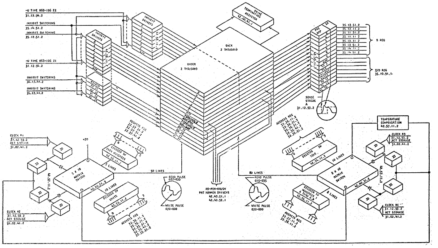
The yellow line shows one of the inhibit drive circuits. The inhibit drive signals come from the processor and are gated for the appropriate timing.
The inhibit drivers
As explained earlier, during the write phase, a 1 will be written to the selected core unless the inhibit line is active. In that case, the inhibit line counteracts the X line; without enough current to flip the core, the core remains at 0. However, the implementation in the 1401 is more complicated than this and there are 21 inhibit drivers in total (16 for data planes, 4 for hole check planes, and 1 for the row bit core planes).
The sense circuit
When a core switches state during a read, the sense circuit must pick up this signal and output the bit value. A key challenge for the sense circuit is detecting this relatively small signal in the presense of large switching signals. The sense line switches direction at the midpoint of each column to avoid picking up interference. A consequence of this is the input signal may be a pulse of either polarity.
The matrix switches
Generating the X and Y select signals is a tricky problem. The drive signals must have a positive pulse of the right current and duration for reading, followed by a negative pulse for writing. In addition, the number of select lines is large (50 X and 80 Y), so hardware costs would be excessive if each line had its own driver circuitry.
The photo above shows the X matrix switch, with 5 row inputs, 8 column inputs, and 40 outputs (connected on the back). The switch consists of 50 cores in a 5 by 10 grid, with 5 lines driving the rows and 10 lines driving the columns. Each core also has an output winding and a bias winding. When two input lines are triggered, the corresponding core flips state, generating a pulse on the output winding. When the input lines are released, the bias winding flips the core back to its original state, generating a negative pulse on the output winding. Thus, the desired one of the 50 outputs has a positive pulse followed by a negative pulse, which is just what the core module requires for read followed by write.
(ILD pages 2 and 3.)
The address decoding circuitry that drives the matrix switch uses an interesting shortcut. You'd expect that the circuit decoding a digit value would use all 4 bits of the digit, but the circuit manages to use a 3-input AND gate for each value. For instance, 2 is detected as not 8 AND not 4 and not 1, ignoring the value of the 2 bit entirely. The trick is that if 8, 4, and 1 bits are all clear, the value must be 2 (keeping in mind that 0 is represented as 10). As another example, 3 is detected as 2 AND 1 AND parity, which is only matched by the digit 3
(ILD page 3).
Physical layout of core memory in the 1401
The following picture (courtesy of
intaretro)
shows the core memory module mounted in its gate 01A1, along with the many SMS cards required for drivers and amplifiers. The gate has Column F at the left, holding the
DKA driver cards and
AQW current source cards that drive the matrix switch boards, and the
AQV inhibit driver cards. Column E is next, holding the
AQU address decode cards.
The address lines plug into the empty sockets at the bottom. Column D holds
WX and
AQX sense amplifiers, and a couple other cards. The core module is mounted with the matrix switch cards on top. At the far right, the empty Column G has connectors for the paddles with the hundreds of wires from the brushes and print hammers.
References
The IBM 1401 core module is documented in detail in
ALD 42. For more information on core memory, see
Coincident Current Ferrite Core Memories
Input Sept 6, 2015